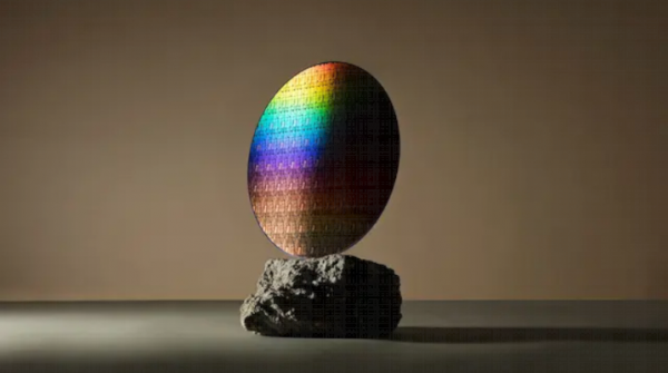
IBM Corp. and Samsung Electronics Co. Ltd. on Tuesday detailed a new transistor architecture that they believe could provide twice the performance of current technology using the same amount of electricity.
IBM公司和三星电子有限公司周二发文介绍了一种新的晶体管架构,两家公司认为这种架构在同样的功率条件下提供的性能是现有技术的两倍。
The architecture is known as VTFET, short for Vertical-Transport Nanosheet Field Effect Transistor. IBM is touting the technology as a “breakthrough in semiconductor design.”
该架构名为VTFET,VTFET是英文纵向传输纳米片场效应晶体管的简称。IBM称该技术是“半导体设计的突破”。
The key innovation in VTFET is that the technology changes the angle at which transistors are stacked on a chip. Normally, transistors are arranged side-to-side such that electricity travels through them laterally. With VTFET, IBM and Samsung have taken a different approach. The technology arranges transistors at a perpendicular angle relative to the chip on which they’re placed such that electricity travels through them vertically rather than laterally.
VTFET技术的关键创新在于,该技术改变了晶体管在芯片上的堆叠角度。通常情况下晶体管是侧向排列的,这种排列下的电流是横向地通过晶体管。而IBM和三星的VTFET采取了一种不同的方法。晶体管是以垂直角度放置在芯片上,电流也就会垂直地而不是横向地通过晶体管。
VTFET could provide several benefits, according to IBM. The transistors on a chip have to be isolated from one another to reduce interference. Chipmakers isolate transistors by placing additional components between them. VTFET removes the need for those additional components, IBM says, which frees up space on the chip that can be used to increase processing capacity.
据IBM称,VTFET可以提供几个好处。芯片上的晶体管必须相互隔离以减少干扰。芯片制造商通过在晶体管之间放置额外的组件来隔离晶体管。IBM表示,VTFET不再需要这些额外组件,因此释放了芯片上的空间,可以用来增加处理能力。
Increasing the available space on a chip gives engineers more flexibility to optimize processor performance, according to IBM. It also becomes easier to improve the processor’s power efficiency.
IBM称,增加芯片上的可用空间令工程师在优化处理器性能方面有了更大的灵活性。提高处理器的功率效率也变得更加容易。
IBM estimates that VTFET technology could theoretically provide twice the performance of scaled FinFET transistors without requiring more electricity. FinFET is the transistor architecture used in most modern chips. Alternatively, IBM says, chip designers could use VTFET to provide a 85% reduction in power usage.
IBM估计,VTFET技术晶体管的性能理论上可以达同比例的FinFET晶体管的两倍,无需更多的功率。FinFET是大多数现代芯片中使用的晶体管架构。IBM还表示,芯片设计者可以利用VTFET减少85%的功率使用量。
IBM envisions numerous applications for the technology. With VTFET, chipmakers might create ultra-efficient smartphone processors capable of extending a mobile device’s battery life to more than a week. In data centers, IBM says, computationally intensive tasks such as encryption could be performed with a smaller carbon footprint. Connected devices would likewise benefit from the ability to perform computations more efficiently.
IBM构想了许多VTFET技术应用。芯片制造商利用VTFET可以打造超高效的智能手机处理器,进而能够将移动设备的电池寿命延长到一周以上。IBM表示,数据中心的计算密集型任务(如加密)可以在较小的碳足迹下进行。连接设备也将同样受益于更有效的执行计算能力。
“Today’s technology announcement is about challenging convention and rethinking how we continue to advance society and deliver new innovations that improve life, business and reduce our environmental impact,” said Mukesh Khare, IBM’s vice president of hybrid cloud and systems.
IBM混合云和系统副总裁Mukesh Khare表示,“今天的技术公告事关挑战传统及重新思考我们如何继续推动社会发展,提供新的创新,改善生活、商业和减少人类对环境的影响。”
VTFET is the second high-profile semiconductor innovation announced by IBM in recent months.
VTFET是近几个月来IBM宣布的第二个备受瞩目的半导体创新。
Previously, the company in May demonstrated the world’s first two-nanometer chip. The technology that powers the chip makes it possible to arrange 50 billion transistors on a processor roughly the size of a fingernail, IBM said. IBM believes that two-nanometer chips could significantly reduce the carbon footprint of data centers and potentially help quadruple mobile devices’ battery life.
此前,IBM曾在5月展示了世界上第一个两纳米芯片。IBM表示,由于该芯片使用的技术,一个大约只有指甲盖大小的处理器上置入500亿个晶体管成为可能。IBM认为,两纳米芯片可以大大减少数据中心的碳足迹并有可能帮助移动设备的电池寿命增加三倍。
IBM is not the only player in the semiconductor market that is developing new ways of building transistors. Over the next few years, Intel Corp. plans to move away from the FinFET transistor architecture used in most modern chips and adopt a newer design dubbed RibbonFET.
IBM并非半导体市场上正在开发新的晶体管制造方法的唯一一家厂商。在未来几年里,英特尔公司计划放弃大多数现代芯片中使用的FinFET晶体管架构而采用一种被称为RibbonFET的较新的设计。
Samsung, with which IBM developed VTFET, is also working to refresh its transistor architecture. Both the technology developed by Samsung and Intel’s RibbonFET are based on an approach known as gate-all-around.
与IBM合作开发VTFET的三星公司也在努力更新旗下的晶体管架构。三星开发的技术和英特尔的RibbonFET都是基于一种名为全方位门(Gate-all-around)方法。
A transistor uses a component known as a gate to manipulate the electrons with which it represents ones and zeros. In the gate-all-around design being adopted by Intel and Samsung, the gate can be customized for different use cases with relative ease. This feature could make it possible to optimize chips for specific tasks to increase performance and power efficiency.
晶体管利用名为门的部件操纵电子用于表示1和0。英特尔和三星采用的全方位门电路设计中的门电路可以相对容易地针对不同的使用情况进行定制。该特点令针对特定任务的优化芯片成为可能,可以提高性能和功率效率。


